






Science & Research
IBM’s 3D Chip Packs 100 Billion Transistors
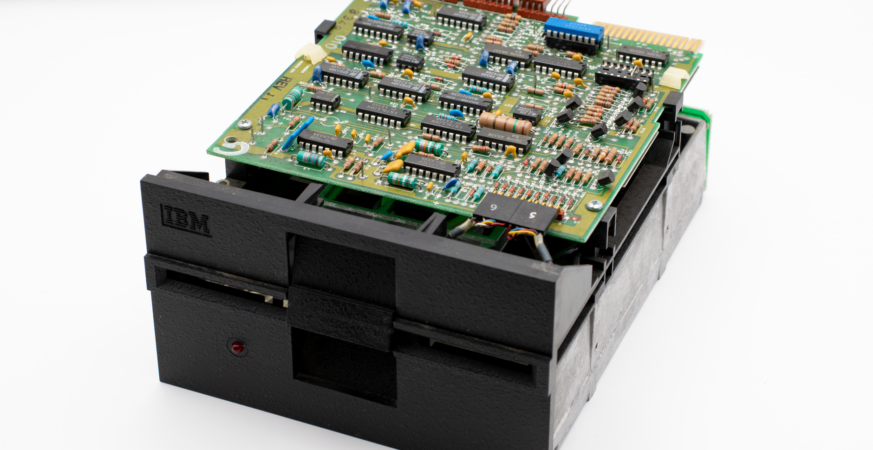
IBM unveiled a 10 mm × 15 mm prototype that crams nearly 100 billion transistors using a three-dimensional technique, promising big gains in efficiency and performance.
WEBSITE: aipostdaily.com
E-MAIL: halilkale87@gmail.com
IBM unveiled a 10 mm × 15 mm prototype that crams nearly 100 billion transistors using a three-dimensional technique, promising big gains in efficiency and performance.
A deep look at ASML’s $400 million EUV lithography system, its 8‑nm resolution, and what it means for chipmakers and developers today.
Independent coverage of artificial intelligence, machine learning, cybersecurity, and the technology shaping our future.
Contact: Get in touch